Research
Wideband Photodetector and Bolometer Devices
We aim to develop a wideband optical detection platform with self-powering capability. We conduct experiments on multidimensional nanostructures to exploit their interface properties. Our research on graphene and carbon nanotube based structures have revealed several significant findings on the role of geometrical importance and interface properties.
Our fabrication facility allows to induce defects sites in the crystal structure or at the interfaces of combined systems together etc. The facility in the laboratory provides a low temperature optoelectronic measurements with wideband source.
Read More
Aluminium coated carbon nanotube film for wavelength-selective surface
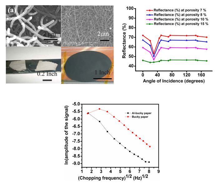
The measured thermal diffusivity of purified CNT and Al-CNT films were 1.63×10⁻⁴ and 1.88×10⁻³ cm2/s, respectively. These results suggest that Al coating has improved the connectivity between MWCNT by reducing the porosity; therefore, it resulted in an improved thermal diffusion as compared to CNT film alone. This higher thermal diffusivity could be additional advantage for the reflective CNT films to dissipate the absorbed heat in the system such as solar collectors.
Reference: APPLIED PHYSICS LETTERS 103, 131909 (2013)
https://doi.org/10.1063/1.4822305
Broadband wavelength-selective reflectance and selective polarization by tip-bent vertically aligned multi-walled carbon nanotube forest
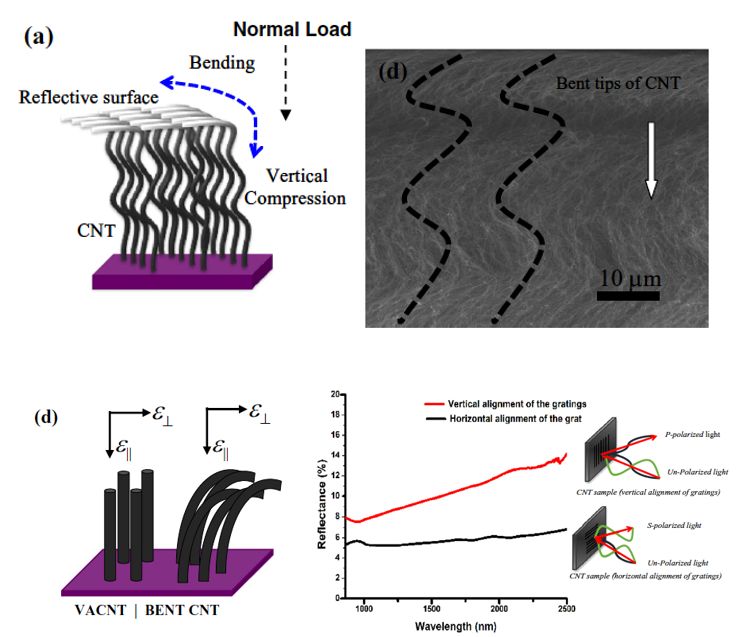
Figure: Schematic diagram of the CNT forest after mechanical bending and compression. SEM image shows a cross-sectional view of the mechanically processed CNTs, revealing buckling along the axial direction of the CNTs (arrow indicates the direction of buckling of the sample and vertical compression). Schematic showing the contribution of the parallel and perpendicular dielectric towards the optical reflectance from the MWCNT and the tip-bent CNT surface. Optical reflectance plotted against incident wavelength to demonstrate a dependence of the optical reflectance on the bending of the CNT forest. The bottom spectrum shows the result from the MWCNT forest and the upper spectrum shows a reflectance from the surface of the bent-CNT forest. Insets show a schematic of the respective samples.
Reference: J. Phys. D: Appl. Phys. 47 (2014) 235501.
DOI: 10.1088/0022-3727/47/23/235501
Nonlinear optical absorption in a graphene infrared photodetector
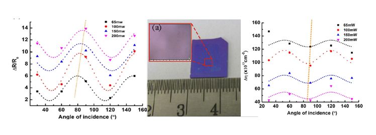
Figure: Optical image of the graphene transferred onto the SiO2 substrate. The changes in the normalized resistance during saturation are plotted with different angles of incidence at various IR powers. change in the carrier concentration is plotted with the different angle of IR incidence for different powers.
Reference: Nanotechnology 25 (2014) 335710.
https://doi.org/10.1088/0957-4484/25/33/335710
Enhanced Photoresponse in Monolayer Hydrogenated Graphene Photodetector

Figure: Schematic of the experimental setup; the source meter is connected to H-graphene placed between gold electrodes, and a variation in the IR incidence angle (30?150°) is shown by arrows. Normalized change in the resistance is plotted with different angle of incidences for different IR powers during saturation. change in the carrier concentration during cyclical experiments with the variation in the angle of IR incidence at different radiation power.
Reference: ACS Appl. Mater. Interfaces 2014, 6, 16763?16768.
DOI: 10.1021/am503892m
Few-layer graphene/ZnO nanowires based high performance UV photodetector
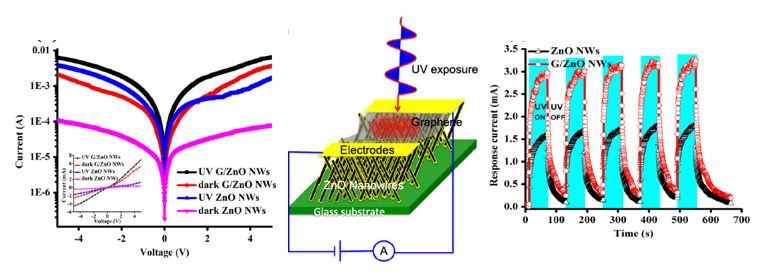
Figure: I–V characteristics of the ZnO NWs and G/ZnO NWs device, where the current is plotted on a log scale and the inset plot shows the current on a linear scale with the applied bias voltage in both the absence and presence of UV illumination. cyclical photoresponses of ZnO NWs and G/ZnO NWs devices upon UV illumination.
Reference: Nanotechnology 26 (2015) 235703
https://doi.org/10.1088/0957-4484/26/23/235703
Highly Dense ZnO Nanowires Grown on Graphene Foam for Ultraviolet Photodetection
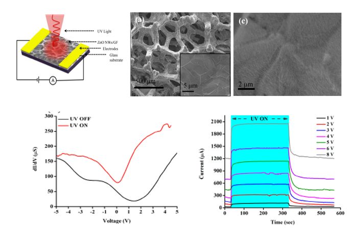
Figure: Schematic of ZnO NWs/GF device. GF at low magnification and high magnification (inset). ZnO NWs on GF. Differential conductivity (dI/dV) of the device plotted with the bias voltage. Saturation experiments at different bias voltage.
Reference: ACS Appl. Mater. Interfaces 2015, 7, 10606?10611.
https://doi.org/10.1021/acsami.5b02403
Photoresponse of double-stacked graphene to Infrared radiation
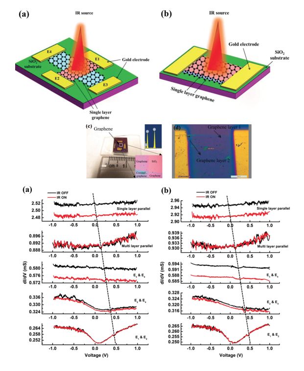
Figure: Schematic of the graphene device: (a) crossed configuration of graphene layers, (b) parallel configuration of graphene layers, (c) and (d) are optical images of crossed- and parallel-layer graphene devices. The insets in figure (c) show a magnified optical image and EDS analysis of crossed graphene layers. Differential conductivity of different graphene samples at angles of IR incidence of (a) 90°, (b) 120°.
Reference: Nanoscale, 2015, 7, 15806–15813
https://doi.org/10.1039/C5NR03676C
Effect of magnetic field on photoresponse of cobalt integrated zincoxide nanorods
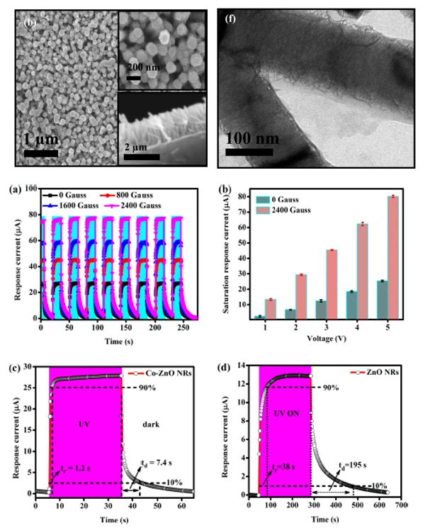
Figure: Co-ZnO NRs. Bottom and top insets in a and b are the high-resolution. TEM images of Co-ZnO NRs. (a) Cyclic photoresponse of Co-ZnO NRs at 5 V bias voltage and (b) variation of saturation response current with bias voltage in absence and presence of external magnetic fields. Determination of response and recovery times of (c) Co-ZnO NRs PD and (d) pristine ZnO NRs PD.
Reference: ACS Applied Materials & Interfaces, 2016, 8, 4771–4780.
https://doi.org/10.1021/acsami.5b11387
ZnO quantum dots and graphene based heterostructure for excellent photoelastic and highly sensitive ultraviolet photodetector
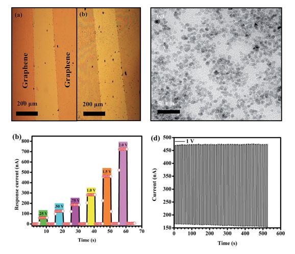
Figure: Optical images of (a) graphene layers on silicon wafer and (b) drop-casted ZnO QDs between the gap. TEM images of colloidal ZnO QDs. the variation of saturation response current with bias voltage at UV illumination intensity of 1.3 mW cm-2. Time-dependent cyclic photoresponse analysis for 54 cycles, where each cycle is for 5 s of UV illumination at bias voltage 1 V.
Reference: RSC Advances, 2015, 5, 90838
https://doi.org/10.1039/C5RA18663C
Sandwiched assembly of ZnO nanowires between graphene layers for a self-powered and fast responsive ultraviolet photodetector
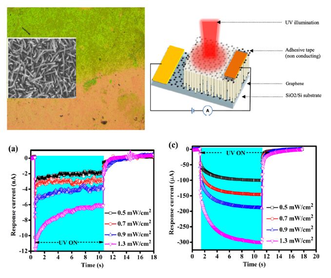
Figure: As-grown ZnO NWs on graphene. SEM images of as-grown ZnO NWs. Schematic of sandwiched heterostructure-based G/ZnO NW/G device. Response current plotted with the time of UV exposure at zero bias. Variation of response current plotted with the time of exposure at -5 V.
Reference: Nanotechnology, 2016, 27, 095205
https://doi.org/10.1088/0957-4484/27/9/095205
Conjugated assembly of colloidal zinc oxide quantum dots and multiwalled carbon nanotubes for excellent photosensitive ultraviolet photodetector
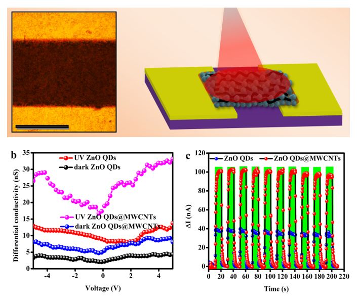
Figure: ZnO QDs@MWCNTs in?between the electrodes. differential conductivity–voltage analysis of both pristine ZnO QDs and ZnO QDs@MWCNTs PDs in the presence and absence of UV illumination intensity of 0.9 mW cm?2. (c) Cyclic photoresponse analysis of both pristine ZnO QDs and ZnO QDs@MWCNTs PDs at 5 V and 0.9 mW cm?2 UV illumination intensity.
Reference: Nanotechnology 27 (2016) 355204
https://doi.org/10.1088/0957-4484/27/35/355204
Energy-Efficient Hydrogenated Zinc Oxide Nanoflakes for High- Performance Self-Powered Ultraviolet Photodetector
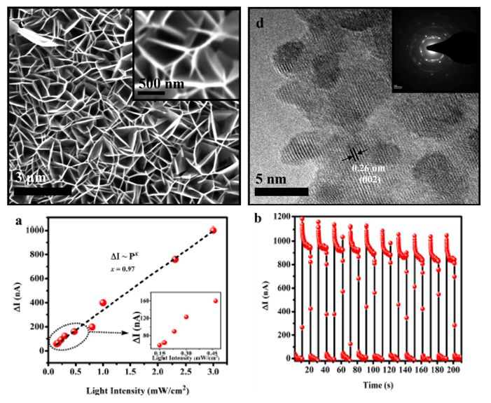
Figure: H:VZnO NFs. (d) HRTEM images of VZnO NF. Dependence of photoresponse of H:VZnO NFs device on the UV illumination intensity at zero bias voltage. (b) Cyclic photoresponse analysis of the device at 3 mW/cm2 intensity at zero bias voltage.
Reference: ACS Appl. Mater. Interfaces 2016, 8, 18182?18188
https://doi.org/10.1021/acsami.6b04954
Surface photo-charge effect in doped-ZnO nanorods for high-performance self-powered ultraviolet photodetectors
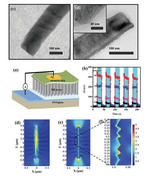
Figure: (a) Schematic of the self-powered UV PD. (b) Cyclic photoresponses of #1: ZnO NRs/PEDOT:PSS, #2: Cl-ZnO NRs/PEDOT:PSS, #3: ZnO NRs/DMSO-PEDOT:PSS and #4: Cl-ZnO NRs/DMSO-PEDOT:PSS PDs. (d) and (e) are the two-dimensional simulated electric field distribution in pristine and Cl-doped ZnO NR and (f ) a magnified image showing the surface of Cl-ZnO NR. (g) LHE of pristine ZnO NRs and Cl-ZnO NRs.
Reference: Nanoscale, 2017, 9, 4536–4543
https://doi.org/10.1039/C6NR07670J
Doping controlled pyro-phototronic effect in self- powered zinc oxide photodetector for enhancement of photoresponse
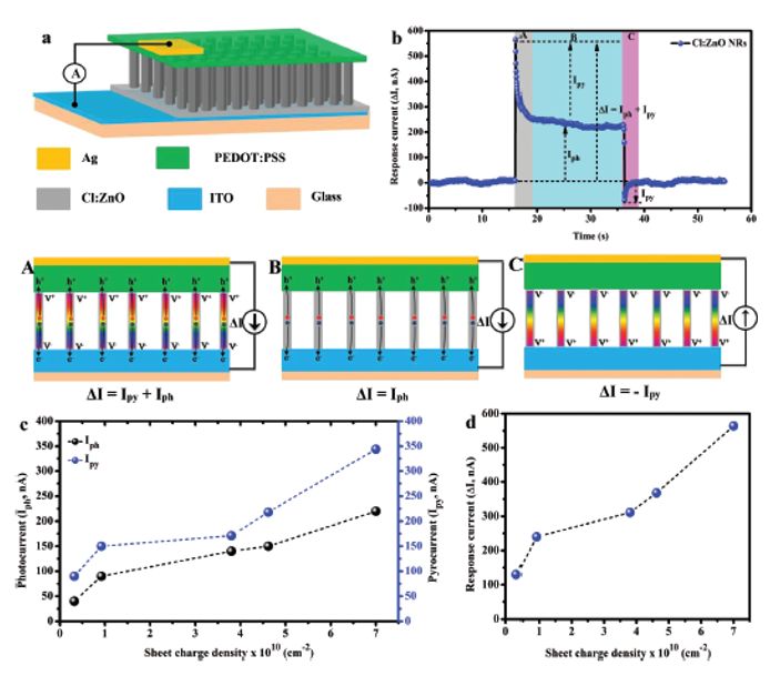
Figure: (a) Schematic demonstration of the self-powered Cl : ZnO NRs PD. (b) Current–time response of the PD under UV irradiation (365 nm wavelength) of intensity, 3 mW cm?2 in the absence of external bias voltage, where UV light was exposed for 20 s. The bottom schematics illustrate the photoresponse mechanism of the self-powered PD at the current-time response stages of A, B and C as shown in (b). (c) Dependence of photocurrent and pyrocurrent with sheet charge density of NRs. (d) Response current plot with respect to sheet charge density.
Reference: Nanoscale, 2018, 10, 3451–3459
https://doi.org/10.1039/C7NR08125A
Spray Coating of Two-Dimensional Suspended Film of Vanadium Oxide-Coated Carbon Nanotubes for Fabrication of a Large Volume Infrared Bolometer
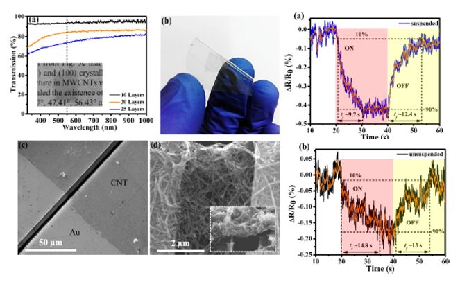
Figure: (a) Transmission spectra of MWCNT thin films for different number of layers and the inset depicts the MWCNT film on the background for transparency. (b) MWCNT film transferred on a flexible PET substrate. (c) SEM image of the MWCNT film on the microfabricated channel on a SiO2/silicon (Si) substrate. (d) Zoom-in SEM image of multiple MWCNT films between the channel and the inset depicts the VCNT film transferred on the channel.Response (tr) and recovery time (tf) calculation for (a) suspended and (b) unsuspended VCNT films at 200 K for 50 ms?1 modulation frequency.
Reference: ACS Appl. Mater. Interfaces 2020, 12, 1315?1321
