Laboratory of Advanced Nanostructures for Photonics and Electronics
Photonics
The lab’s primary focus lies in exploring advanced nanostructures, specifically gallium-based metal nanostructures on flexible PDMS and dielectric metasurfaces, with thorough investigations aiming to showcase their applications in three main fields: displays, imaging, and optical instrumentation.
Displays:
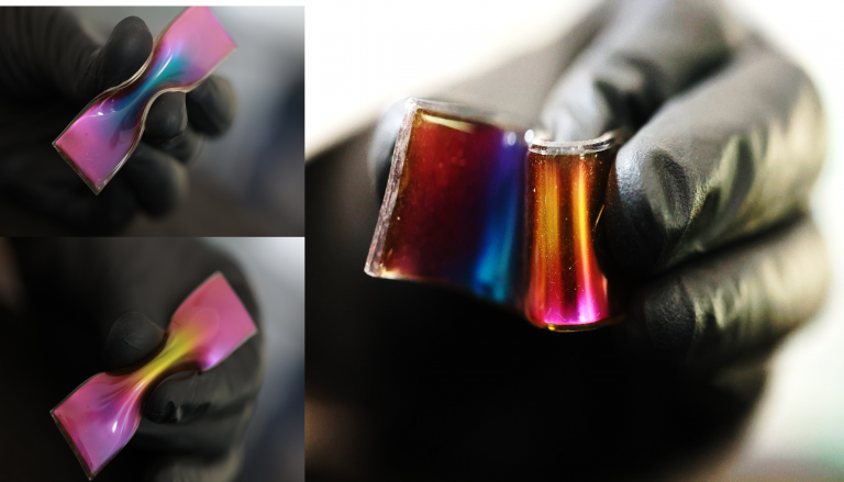
Ga based nanostructures:Liquid metals, such as Gallium, have been used for electronic applications but widely in the photonic domain due to their inability to be scaled down to the nanoscale. In this work, we have developed a single-step procedure that exploits fluid instabilities to form sub-100nm sized non-coalescent nanodroplets of liquid metal on a substrate, enabling the fabrication of gallium-based plasmonic thin films with tunable structural colors rendered via gap-plasmons. This technique has potential applications in reflective display technologies and mechanochromic sensing, offering opportunities for dynamically reconfigurable thin-film-based functional nanodevices in situ.
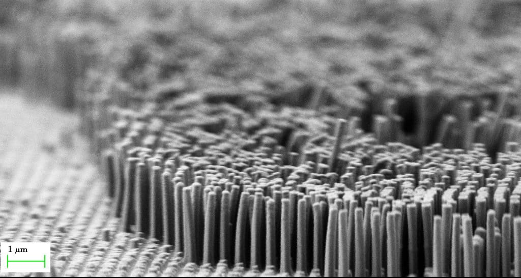
Extreme aspect ratio all polymer nanostructures: Low-index flexible polymers require high-to-very-high aspect ratio nanostructure to exhibit their optical properties. Therefore, a method to achieve nanopillars with an aspect ratio of more than 10 is being investigated, particularly showing its applications in metasurface based filters and lens.
SEM images of High aspect Ratio nanostructures
Metasurface based holography: The lab is also interested in demonstrating the potential of metasurface-based holography for futuristic applications, such as dynamic displays, optical security, and other applications that require the manipulation of light,
Imaging:
Achromatic Metalens: The objective is to control the chromatic aberration of the image by controlling the size and shape of the nanostructures in the metasurface, hence to achieve an achromaticity in the specified bandwidth, which in this case is the visible, mid-wave infrared (MWIR), and long-wave infrared (LWIR) spectra.
Wide Angle Metalens:
For imaging applications,we need wide angle field of view(FOV).To acheive this we explore various ways to arrange the nanostructures to get highly efficient wide angle metalens.
Super resolution Metalens:
In mathematics, a function can oscillate faster than its highest fourier component.This can be incorporated in optics to get higher resolution than the resolution given by abbe’s diffraction limit.We are interested in various methods to acheive super resolution to image objects in nanometer scale.
Optical Instrumentation:
3D printing with Metalens: The arrangement of meta-atoms can be used to control the shape of a beam of light. This can be done by carefully designing the size, shape, and spacing of the meta-atoms. By controlling the shape of the beam, it is possible to create beams with a variety of shapes, such as needles, squares, triangles, and rings. These beams can then be used to print various shapes of nanostructures with different aspect ratios.
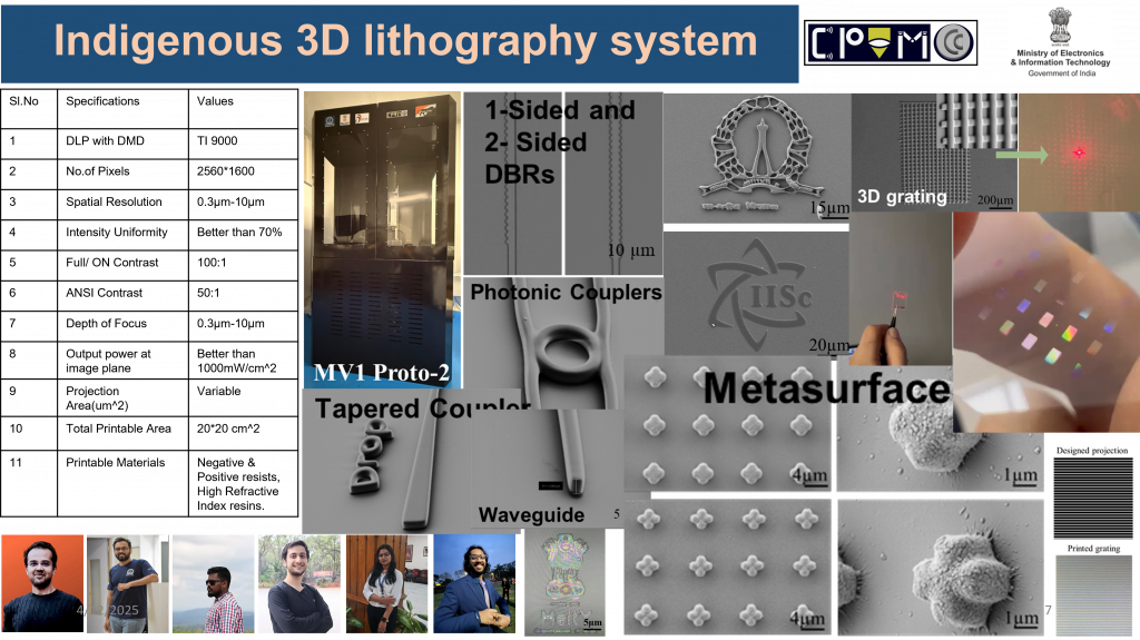
Indigenous sub-micron resolution 3D printer: We work on developping multiscale, multi-material fabrication platform that combines lithographic patterning with droplet-on-demand (DoD) material deposition for applications in optics, electronics, and packaging. Traditional methods, such as photolithography and droplet-based printing, often struggle to achieve high-resolution 3D structures, multi-material integration while maintaining scalability. This hybrid approach leverages mask/maskless lithography, photolithography, direct laser writing, and nanoimprint lithography (NIL) for precise nanoscale features, while DoD techniques such as inkjet, aerosol jet, and electrohydrodynamic printing (EHD) enable controlled deposition at micro- to millimeter scales.